Turn a KiCAD Schematic into a PCB
In this jam, we will turn our schematic from Part 1 into an actual PCB layout.
This Jam is in BetaWe need your help and feedback on the clarity of this jam.
Prerequisites
The rest of the workshop assumes you understand PCB Basics like:
- Traces: A continuous stretch of copper that connects multiple parts.
- Layers: Layers are parallel surfaces of stuff on your PCB. There are a bunch of different kinds of layers, like:
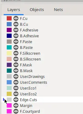
KiCAD Layers: 1
F.Cu/B.Cu: The layers of copper on your PCB. The conductive traces on your board should live on these layers. Separate conductive traces can not cross each other on the same layer, you must use a via to connect two layers and not cross traces on the same side of the board.
F.Silkscreen/B.Silkscreen: The printed (silkscreened) layers on your PCB. These are either white or black and must be monochrome (you can't have gradients, everything must be a clear line). Anything can go on these layers, they are simply printed.
F.Paste/B.Paste: Anything that will be soldered needs to have paste on it. You probably don't need to mess with this layer unless you know what you're doing, it should be automatically handled by your part footprints.
F.Mask/B.Mask: The soldermask is the colored coating that goes on the board. By default, it covers everything except pads and is what gets printed on. Removing soldermask can be used to expose copper for cool effects.
Objects > Ratlines: These have no impact on the final production of your board, they are simply guides to tell you where you still need to draw traces.
Edge.Cuts: This is the actual outline of how your board will be cut.
User.Comments: This layer has information that will not be printed on the board and is only visible in KiCAD. Think of it as comments in your code.
Reminders:
- Make sure you draw your traces! You shouldn't have any ratlines on your board when you send it for production.
- Remember separate conductive traces cannot touch each other.
- You can use a combination of layers to design the look of your board.
- You almost always want to have the traces of your board covered with soldermask, but it's typically ok to have other copper regions exposed, just remember it might tarnish.
- JLCPCB engineers will review manufacturing details of your design before production, if they spot any issues they'll send you an email to check it. However, don't rely on this to catch circuit issues.
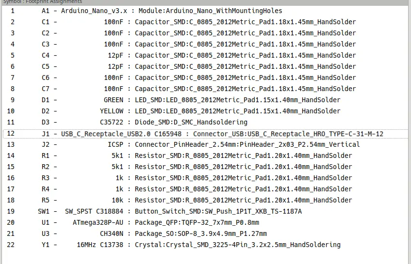
Footprint assignment
Footprints are the exposed copper pads on the PCB for each component. They represent the physical size and shape of the components.
First, click on 'Run footprint assignment tool'.

In the new window, under Footprint Filters, select the first one - "filters defined in symbol" - but deselect the other two.

Now, you should have a window like this with some footprints autofilled, others empty.
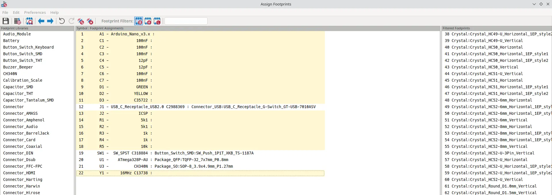
Some footprints, like the Arduino Nano outline, which is not a real component in this case, only have a few options. Double-click on Module:Arduino_Nano_WithMountingHoles to select it.

Generics
0402, 0603, 0805, and 1206 are common sizes of small two-terminal SMD components like resistors, capacitors, and diodes. 0805 is very common and somewhat convenient to place by hand, so we will use 0805 for all our components2.

To find our first capacitor, go to jlcpcb.com/parts. In this case, we will search for 100nF, our first capacitor.
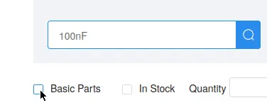
Then, scroll down and select "Basic Parts" to find the parts that don't have the extended fee and we see that they do have 0805 available. So, click on the component and search for 0805 in footprint selection. Do this for each component.
You should find that all of the components have 0805 parts available and in stock.
Specifically, all capacitors will be: Capacitor_SMD:C_0805_2012Metric_Pad1.18x1.45mm_HandSolder3
all LEDs will be LED_SMD:LED_0805_2012Metric_Pad1.15x1.40mm_HandSolder, and all resistors will be Resistor_SMD:R_0805_2012Metric_Pad1.20x1.40mm_HandSolder.
Specific Components
If you look up the Diode C35722, you will get its LCSC page, which says the package is SMC(DO-214AB).
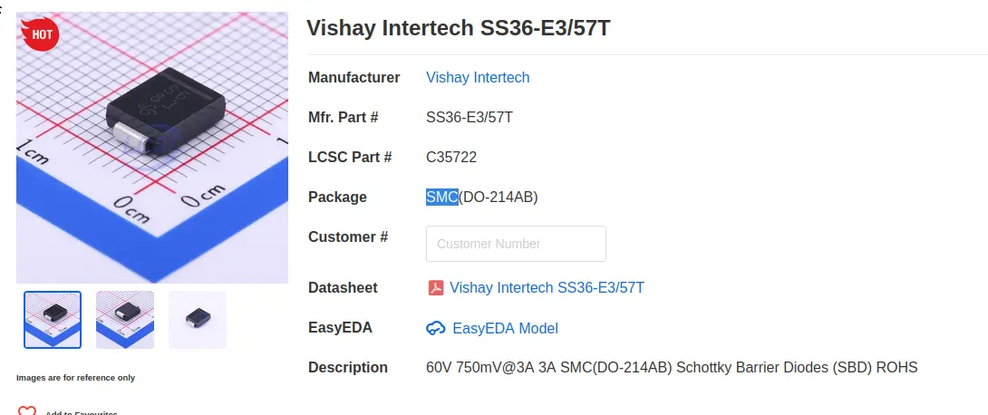
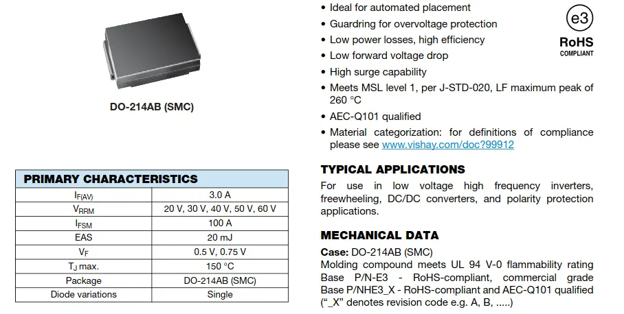
Going to the Datasheet also confirms this.
Then, in KiCAD, after selecting the diode, we can search for the package. While there are no results for DO-214, SMC shows up and we can select Diode_SMD:D_SMC_Handsoldering.

Do the same reseach with the Crystal to get the footprint/package.
Did you try it yourself? Click here for the Crystal's footprint.
Looking up the part number, C13738, for the crystal on jlcpcb.com/parts should give the package, SMD3225, which is the KiCAD footprint Crystal:Crystal_SMD_3225-4Pin_3.2x2.5mm_HandSoldering.
Similarly, for the ICSP header, you will get the right result by searching for 2.54mm (i.e. 0.1 inch pin spacing), and 2x03 (6 pins arranged in 2x3): Connector_PinHeader_2.54mm:PinHeader_2x03_P2.54mm_Vertical.

Other components
You might've noticed that my original footprint assignment window had some components filled out already. This is because chips like the ATmega328P-AU only have one footprint - that's what the AU designates.
Others, like the switch, were found by searching for their part number, 1187A, in the footprint window.
Lastly, some components like the USB-C Receptacle can be weird. While there are hundreds of different manufacturers of USB-C ports and receptacles, there are only a few common designs. However, there is no way to confirm which part uses which design without manually checking each dimension, so I just used the popular HRO_TYPE-C-31-M-12.
Now that our footprints are all selected, we can move on to the PCB!
PCB
Setup

Click 'Open PCB in board editor' in the schematic view.
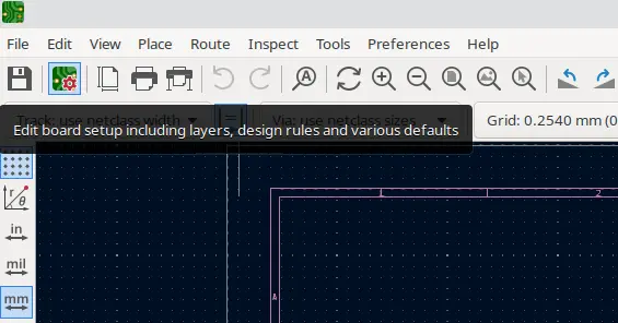
In the PCB editor, click on 'Edit board setup'. This is where we will set the constraints of our design.
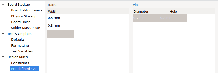
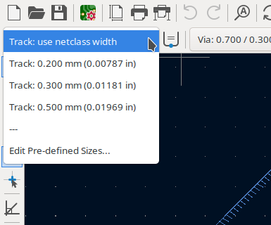
Then, in Design Rules > Pre-defined Sizes, specify how wide you want your traces, vias, and differential pairs will be. KiCAD will let you pick between the options here when designing your board. We will set a track width of 0.3mm for signal traces, 0.5mm for power traces, and 0.7mm diameter vias with a 0.3mm hole4.
Then, press OK to save and exit board setup.
Set Up Components
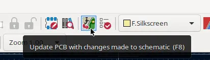
Now, in the board editor window, clicking on 'Update PCB with schematic' brings in all your components to the PCB page. If you make schematic changes, you can click on this to bring in your new parts. In the Update PCB window options, check Delete footprints and Replace footprints and click on Update PCB.

Place them off to the side for now.
Board Edges
Now, to define the edges of our board, select the Edge.Cuts layer in the layer menu.
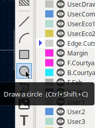
You can use the shape tools to draw the outline of the board, or...

you can go to File > Import > Graphics to import a custom SVG. You can pick whatever shape you like here.
Note: In part 3 of this jam, we will be adding more features such as an LED strip and accelerometer to make a level. Make sure your design will support the physical realities of being a level, such as having two points to balance on, which do not have any ports. Also, consider how your LEDs will physically and aesthetically fit. Make a rough paper sketch if that helps. Of course, none of this applies to you if you have different plans for your board.
By default, your drawing probably won't fit the Arduino Nano template.
Delete the first import and go back to File > Import > Graphics. Play with the scale setting until your design snugly fits the Arduino Nano template (while leaving space for other components).
This step will take some trial and error.

Clean up the drawing to only leave one continuous board shape.

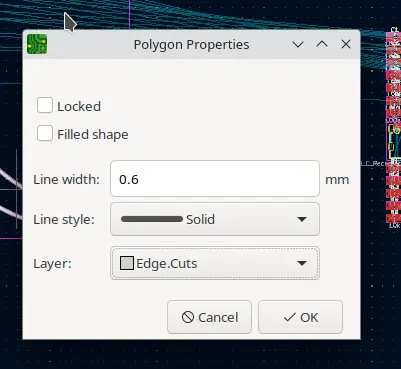
Double-click the shape and set it up like the image above.
- Not Locked
- Not Filled
- Line width: 0.6mm
- Line Style: Solid
- Layer: Edge.Cuts
In case you don't have a nice SVG, but do have a solid shape image, try KiCAD's Bitmap to Component converter. Paste the Footprint into your PCB design, Right Click > Edit Footprint, and follow the above steps.
Components
Note: Many of the choices in this section will depend upon your outline. Feel free to ask for help in #onboard-help on Slack.

After you position the Board Edge and Arduino Template, lock them in place (Select Both > Right Click > Locking > Lock) to avoid accidentally moving them.
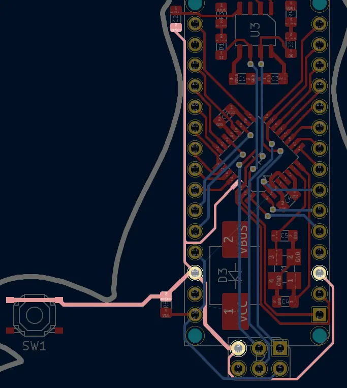
Then, start placing the major components: USB Port, ICs, Microcontroller, buttons, etc.
Have your schematic split screened with the PCB layout. Whenever you click on a component in one, it will be focused in the other. This way, you see what passives5 go with which major components and you can place them logically near each other. The decoupling capacitors for an IC must be right next to it.
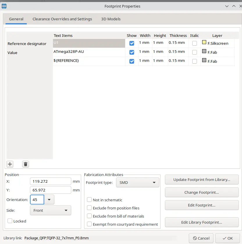
Rotate them to a position that'll make running traces convenient. For example, you want the D+ and D- pins of the USB controller to be facing the port, and the TX, RX pins to be facing your microcontroller. You can rotate things 90 degrees by pressing 'R' on your keyboard, or set a 45 degree offset for the MCU by going to properties.
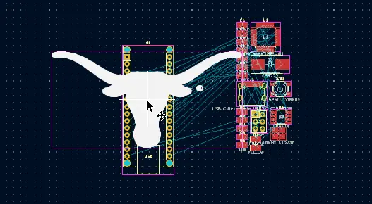
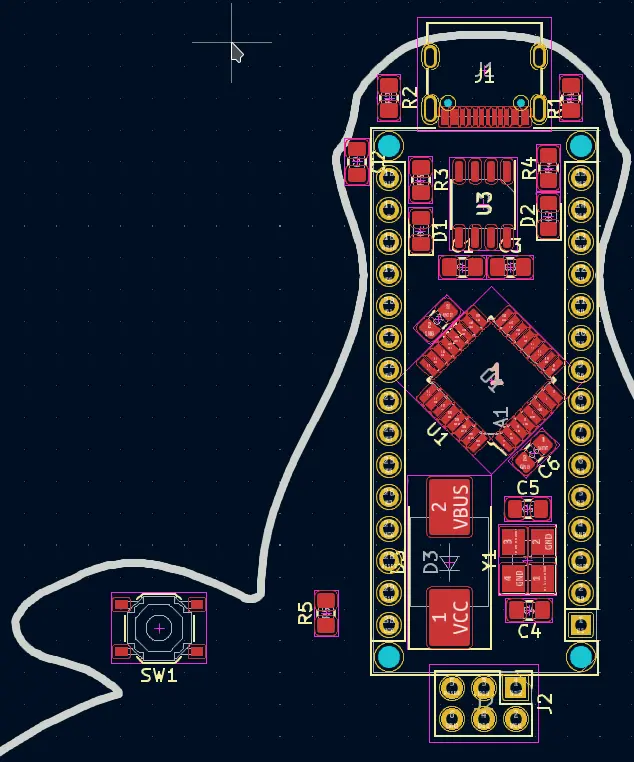
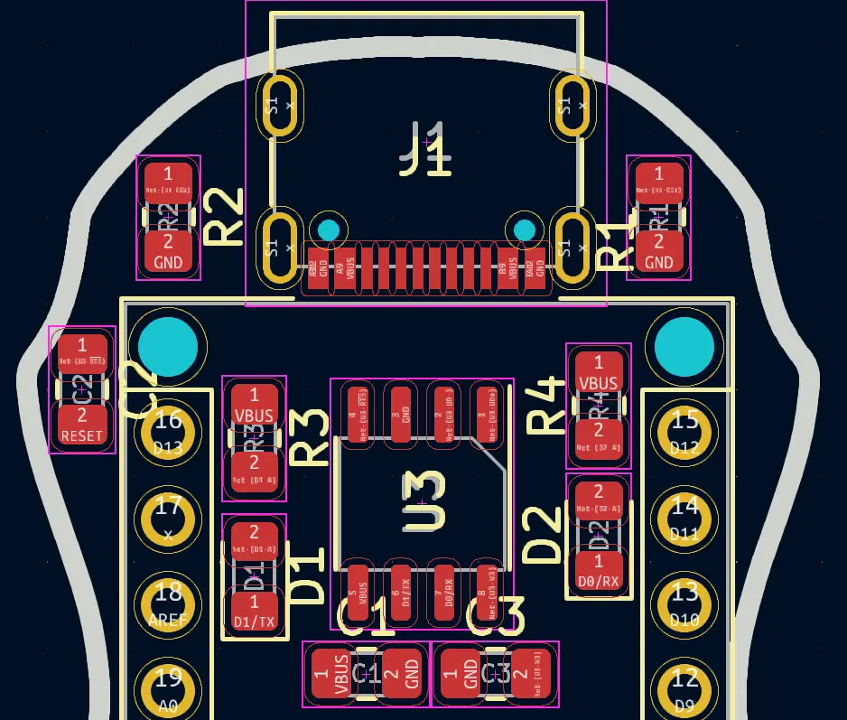
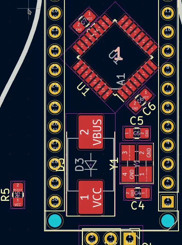
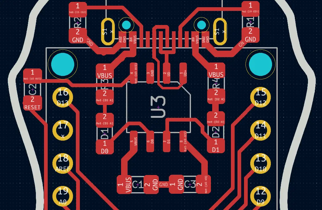
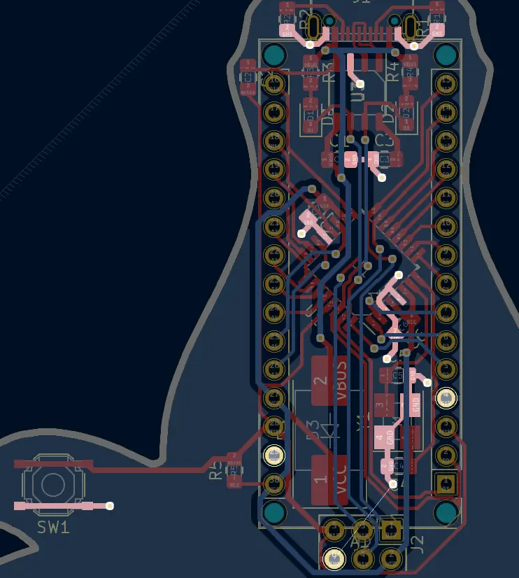
This is how I roughly laid out the core components within the Arduino Nano footprint. Some large components like the reset switch and diode are outside the main nano footprint. The red pads indicate that these are all on the F.Cu layer. This is the front of the PCB. While a typical Nano design needs to be two-sided (have components on both the front and back) to fit within that footprint, here, we will make a larger, one-sided board to keep assembly costs down.
You have to be clever and very deliberate with the placement for your components so minimize the amount of wiring going around other things. Spending a little bit more time on this step will make your routing life sooo much easier. Take inspiration from my layout, but you can't just copy it becase my reference numbers are different. Look at the schematic and see which component connects to what.
Note: This layout took several rounds of iteration between layout and trace routing to generate. It's absolutely fine, and in fact, necessary to come back to rearrange your components if you find your layout doesn't work when routing traces. If this is your first complex board, you'll quickly find that learning routing is the most tedious part of your board, but obviously necessary to get your board working.

While laying out your board, the 3D viewer is a very useful tool. Use "Alt+3" to open it.

If some components are not visible, go back to your board design and double-click the part to open properties.

Make sure you're in properties for the whole component, not just one pad or silkscreen, and then open the '3D Models' tab. Click on the file browser for the 3D model line. These are the correct models:
- USB Connector:
${KICAD7_3DMODEL_DIR}/Connector_USB.3dshapes/USB_C_Receptacle_GCT_USB4105-xx-A_16P_TopMnt_Horizontal.wrl - CH340N:
${KICAD7_3DMODEL_DIR}/Package_SO.3dshapes/SOIC-8_3.9x4.9mm_P1.27mm.wrl - SW1:
${KICAD7_3DMODEL_DIR}/Button_Switch_SMD.3dshapes/SW_SPST_TL3342.wrl
These may vary based on your version of KiCAD.
Routing
To route tracks, follow the Ratsnest (thin blue lines connecting matching nets), and connect the pads. Look at the schematic to see which parts should go where. Start with data signals, and do power and ground later. An efficient layout, one that uses less wires, is often the mostly aesthetically pleasing too.
Try to use the higher thickness 0.5mm trace for sensitive applications like the decoupling capacitors, clock, power lines, etc if you can fit it, and 0.3mm for regular data lines4.
The following images are how router the traces:
Note: You can press "x" when hovering over a pad to start a trace.
In the Appearance sidebar go to Objects > Locked Item Shadow, and hide it to clean up your layout a little bit. Feel free to play with the opacities of other elements to get to a point that you are comfortable with.
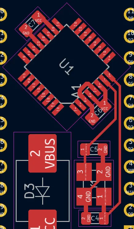
The purple lines are the 'Courtyard' - they show you how close two components can be without physically interfering, so, you keep the decoupling capacitor and IC's courtyards very close to each other.
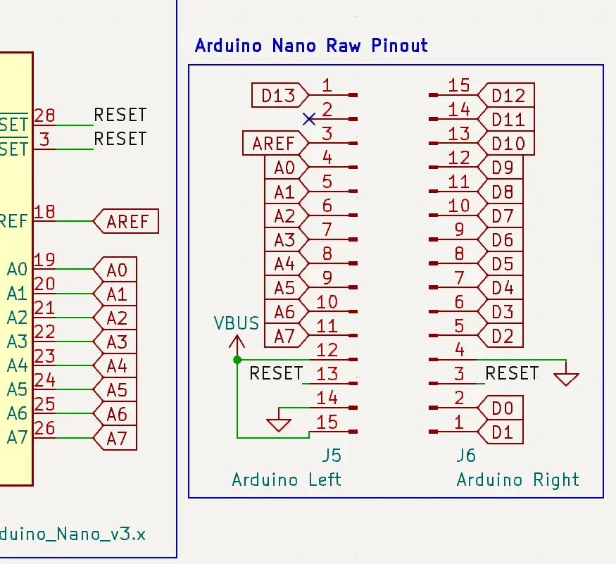
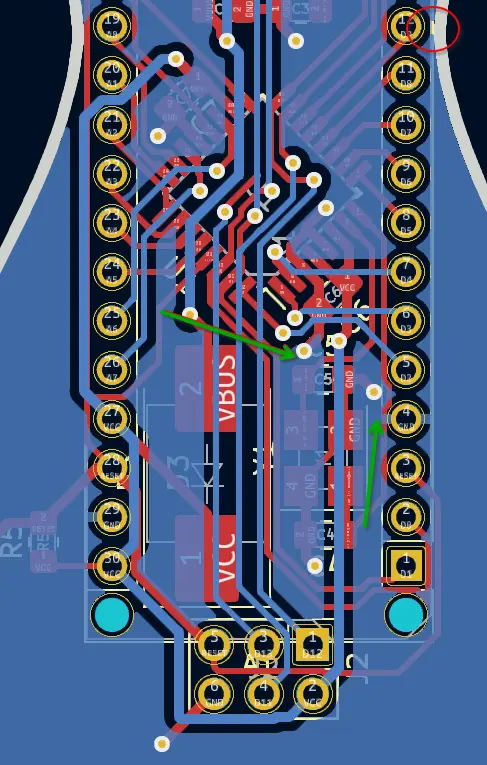
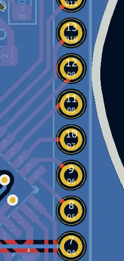
And then, connect the microcontroller pins. In my layout A0-A5, D0, D1, D5-D13 can be routed on the top layer as shown above.
I have to emphasize, this is just what I came up with. This is not the right layout, this is not the best layout. It's one out of the infinite possible arrangements of these traces.
Two-layer routing
Now because there is no way to connect D4 of the microcontroller to the header pin, we will have to jump layers. A via is a tiny hole in your board that connects traces on two sides. It's drilled into the PCB and filled (or plated) with copper to connect the two sides.
First, press 'X' to start running a trace away from D4, towards the inside of the microcontroller.

Move to some empty space then press 'v' to create a via.

Click to place the via, and now you can drag a blue trace - on the back side of the board.
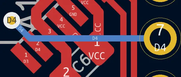
Click on D4. Since D4 and other pins are through holes, you can connect traces from either layer to them.
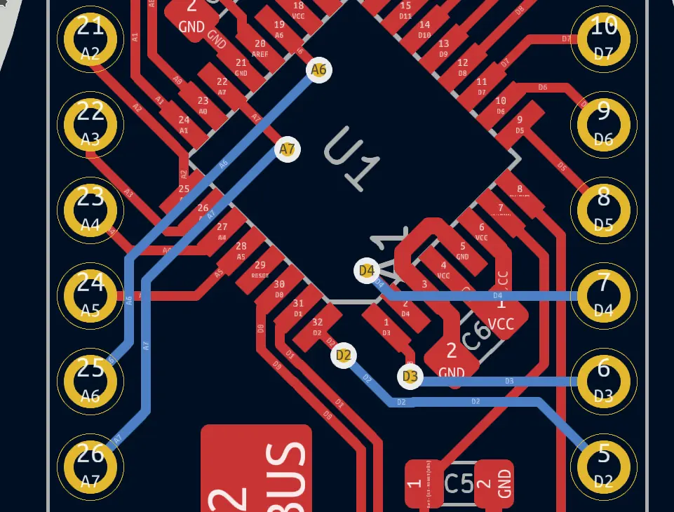
Just like D4, use vias on A6, A7, D2, and D3 to reach their respective header pins.
- If your via is too close to a pad, solder might flow into it and prevent the pad from being properly attached. So, even though KiCAD doesn't stop you from doing that, stay a safe distance away from pads.
- Note how this uses vias to cross A6 and A7. This prevents us from having to run A7 all the way outside the headers to loop around.
You can click on the blue B.Cu layer in the Layers sidebar to visually bring the back layer traces to the front.
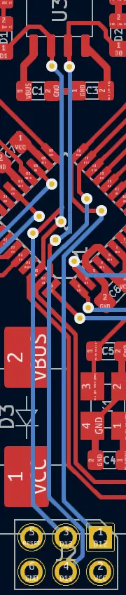
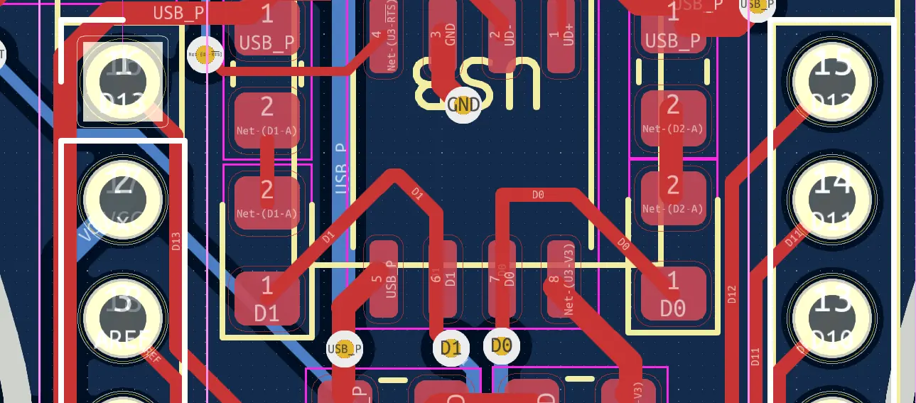
Just like that, use vias and thoughtful crossings to connect D0/D1 to the USB chip and D11/12/13 to the ICSP header. However try to minimize the length of traces on the back, because of the ground plane we will later put in.
The other tracks
And then you can run the Reset track.

And VCC.
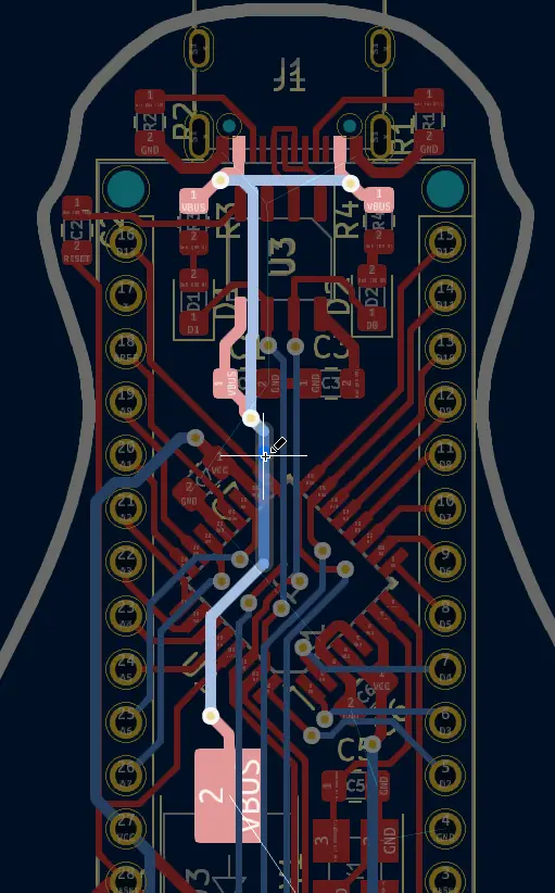
And then a little bit of finagling with the A6, A7, and D13 vias lets us run VBUS under the Microcontroller, straight up to the USB port.
Now, we only have ground pins left, and for that, we'll do something special.
Ground Plane
A ground plane is a large continuous chunk of copper on a layer. It creates a low impedance i.e. clean and easy path for ground current to return. (Because physics) Having an adjacent ground plane also reduces the interference between parallel traces. More complex 4 layer boards might even have a plane for VCC power. In this board, the ground plane will take up all the unoccupied space on the B.Cu layer.
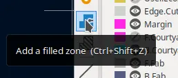
First, click on 'Add a filled zone'.

Then, click on a point far outside the edge of the board and set up the Copper Zone to be connected to ground, and to remove islands below 10mm^2.

Then, draw a shape encompassing the whole board and press 'B' to build the plane.
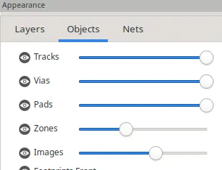
You should play with Zone opacity in the Objects sidebar to find something good for you.
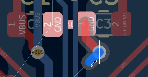

Then, start dropping vias from ground pads. Press escape when it draws a blue trace, you only need the via here.
The through-holes should connect themselves to the ground plane. This is what all the grounds look like.
(Optional) Header Pins
If you want your PCB manufacturer to install Arduino Header Pins on your board.
This could be useful if you want to mount your board onto a breadboard but don't have soldering equipment.
Go back to your schematic and add these two Conn_01x15_Pin symbols and connect them to the correct nets.
Note how D0/D1 are flipped relative to the rest of the pins.
In the footprint selection window, select PinHeader_1x15_P2.54mm_Vertical for both.

Update your board to sync it with the schematic and then position the new pins on top of the old ones.
 You might have to zoom in to get the holes perfectly concentric.
Lock the new pins in place (Right Click > Locking > Lock) and delete the old Arduino layout.
Additionally, you might want to add pin labels on the back silkscreen layer (where there is more space).
Design Rules Checker
Note: This section will vary a lot for you based on your design and layout.
The Design Rules Checker (DRC) looks at the constraints we set the board up with and finds problems in the design.
After you run the DRC with Refilling and Parity checks, you should see a bunch of errors.
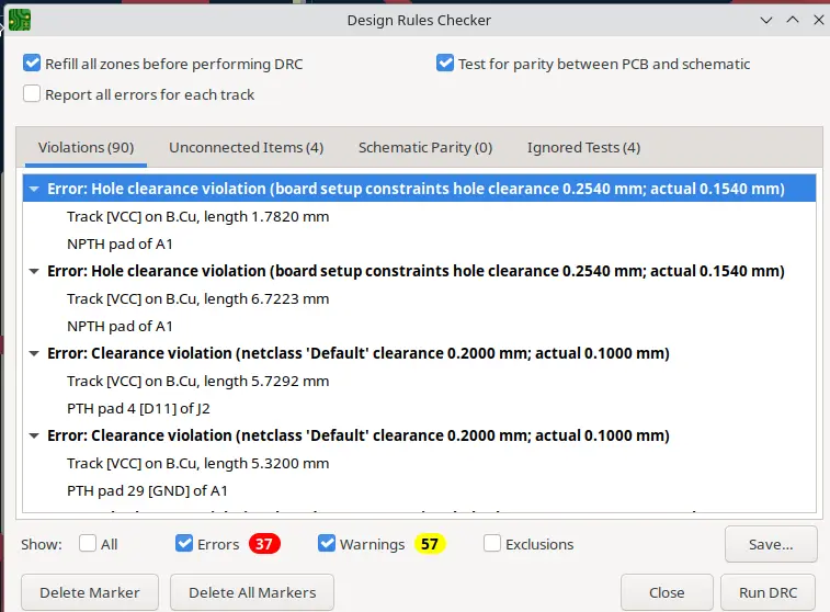
Sooo, there's 90 issues. That's not good. Luckily, the vast majority of them are inconsequential.
The most important issues are in the Unconnected Items tab:
- All 3 unconnected SHIELD errors can be Right Click > Excluded. Microcontrollers and complex ICs might have multiple pins that serve the same function, so KiCAD expects identically named pins to be interconnected. In this case, it's meaningless and can be ignored because it's just the USB housing.
- GND on the ICSP header is disconnected. That's a big problem.
Note: while this solution is presented straightforwardly - coming up with it really wasn't. I spent way more than 30 mins comparing approaches before I decided on this.
Turned out, the part of the ground plane that connected to this GND pin was disconnected from the rest 6, so make it like this:

The ground plane island highlighted another issue with this design. If you follow the current flow from the USB port to the bottom plane, it turns out the whole thing relies on one .3mm connection under the clock.
Fortunately, there's an easy solution: double-click the ground plane to open properties and change its clearance and minimum width to .3mm.

Then, the ground plane goes in between the planes and it's a continuous chunk again.
And now our board is electrically done!
You can solve other DRC issues pretty easily.
- For trace clearance issues, just move the trace away from the specified component. These sometimes pop up when rearranging components.
- You can ignore/exclude all the Courtyard Overlaps with A1. That just points out that there are components inside the Arduino template 7.
- Through-hole has 'Thermal relief connection incomplete': if the connection looks good enough, it's good enough.
- Ignore most 'Footprint doesn't match copy' and Silkscreen warnings. Manually fix the silkscreens that you want to see.
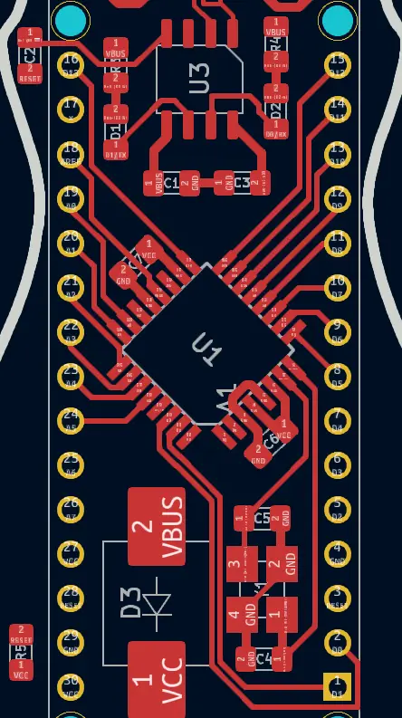
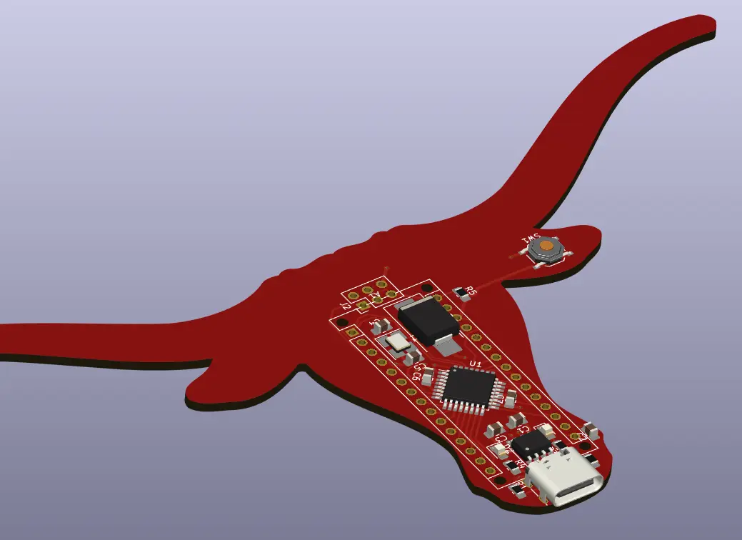
Finished Board


Footnotes
-
Tips in prerequisites by @camdan.me. ↩
-
More info at https://eepower.com/resistor-guide/resistor-standards-and-codes/resistor-sizes-and-packages/# Also, we're only using 0805 in Part 2, not Part 3. ↩
-
These HandSolder footprints do not mean that you have to hand solder them. JLCPCB will still assemble these components for you. HandSolder footprints simply give you more space under component - just in case you need it to fix stuff. Picking the non-handsolder versions of these footprints is perfectly fine. ↩
-
These sizes are just arbritary sane defaults. The point I'm illustrating is that your power traces should be big to reduce their resistance, and signal traces can be smaller. Things get more complicated if you're doing AC power, RF or audio signals, but that's way beyond the scope of this jam (and my knowlege :)). ↩ ↩2
-
Resistors, capacitors, diodes, etc. In this context, equivalent to minor/support components. ↩
-
Ideally, the ground plane would be a continuous, mostly unobstructed chunk, but that would require either spreading out the components or more layers. Both would result in more complexity and cost, which is not good for this workshop. ↩
-
If you're obsessed with details like me and want to fix it, right-click A1 > Open in Footprint Editor; delete the purple courtyard. This only affects this one instance of the Arduino footprint, and won't affect future PCBs you make with KiCAD. This tells KiCAD that the Arduino is not an exclusive component, and other things can overlap it. ↩
Congratulations! 🎉 🎉 🎉If you're a highschooler who enjoys programming or tinkering with hardware, make sure to join Hack Club, the world's largest nonprofit empowering teenagers to make cool projects! There's tons of programs where you can get prizes for programming, get your hardware projects fully funded and you can join the awesome community of 100k+ teenagers who love making cool stuff (just like you!).