Get familiar with PCBs + Make a blueprint!
Want to just see the result? See the Schematic and the EasyEDA source.
Putting the "scheme" in schematic

Has this ever happened to you? You really need a USB hub!
Today we're going to make a USB splitter. It'll have 1 USB-A on one side, and 2 USB-A ports on the other side. It can transmit power as well as data.
We're starting with a schematic. They're like the blueprint for a PCB. It's a good way to figure out what's connected to what before you actually lay out the parts on your board.
Schematics correspond to the parts of your PCB.
Start a new project
Go to EasyEDA and create a new project (File > New > Project...). Name it usb-hub.
Add the parts
For our design, we're going to need a USB-A connector that plugs into our computer. Click the Libraries button on the left toolbar, and search for C98125.
Once you select it, click the Place button to add the part to our project. It might look a little different than the images in this tutorial, but that's okay.

Yeah! You did it. Now let's add the other parts we'll need!
We'll need another USB-A connector, but this time a female connector for the devices we charge / plug in. Do another search for usb-a. A bunch of options will show up with options like price, stock, and mounting type. You won't understand all the options yet & that's ok! I ended up using part number C46407. This time, place 2 of them on the board.
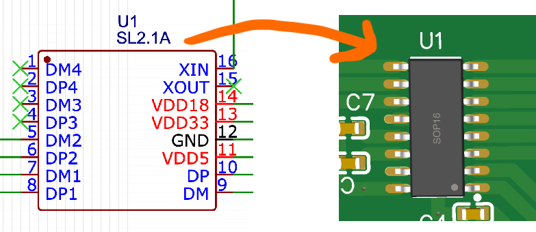
Next up we need a main board to connect everything together. There are a bunch out there, but I ended up using the CoreChips SL2.1A with part number C192893.
Now that we've got a great big pile of parts in our sandbox, the next step is to connect them together!
Connect it together
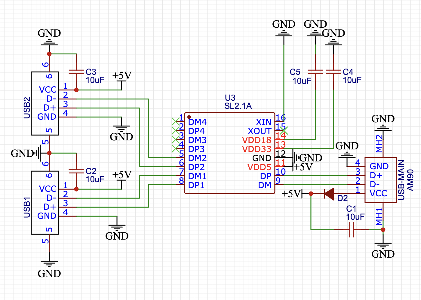
We've got a whole list of parts to hook up now. Let's start with the USB-A male connector to the CoreChips SL2.1A. But what do we need to wire together?
Connect it together Read the spec!
Read the spec!
Let's find the spec for the CoreChips SL2.1A. A spec is kinda like a README for a part. Every part has one, and it's a great place to start when you're trying to figure out how to use a part.
Go to lcsc.com and search for C192893. Click on the part and scroll down to the Datasheet section. Click on the link to download the datasheet.
Just in case, here's a link to the spec sheet for the SL2.1A.
Now let's open it up and just start reading through the table of contents to find where whoops wait it's all in Chinese.

That's fine! Many specs are in other languages and guessing/translating is part of the skill! The important part is in here, the list of pins and what they do. It looks like this:
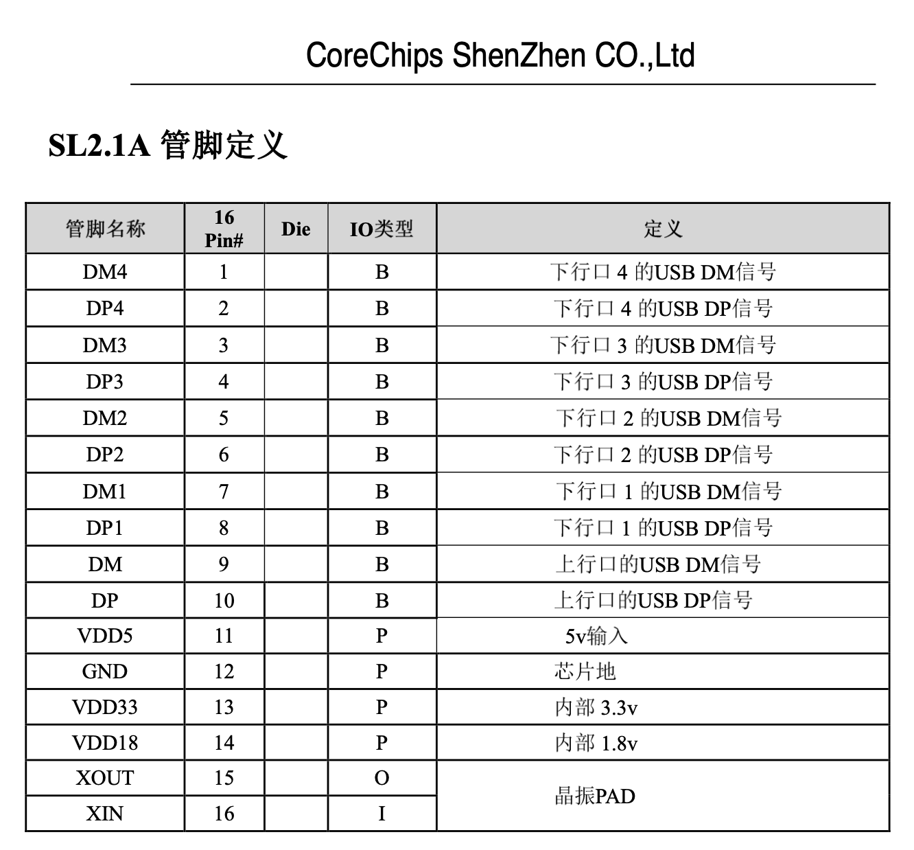
Printed Circuit Board (PCB) part-makers really like to use acronymns, which are the same in every language! We can use the acronymns to figure out what the pins do. Here's a list of the ones we'll need:
- VDD5: 5V power (also called VCC or VBUS)
- GND: ground
- DP: data positive (also called D+)
- DM: data negative (also called D-)
Great, now we know what we need to do on the chip side, let's find the spec for the USB-A!
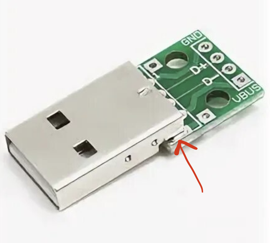
The part I chose also had a spec in chinese, but it's a common part so I found this by googling "USB-A pinout spec". It's a bit different than our pin numbers, but the names are the same. The only difference is that our ports HM1 & HM2 are also GND ports. You don't need to know why right now, but for the curious, google "grounded USB shield".
Connect it together, for real this time!
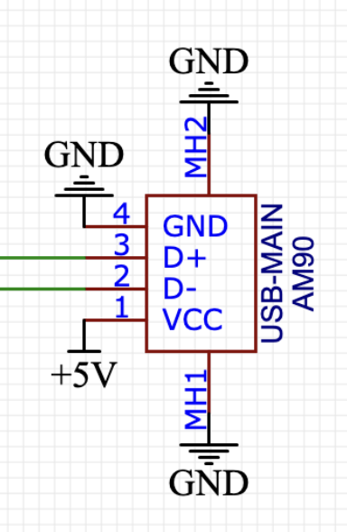
Move the parts around so they're facing eachother (you can rotate them with the R key), the go ahead and connect GND on the usb to GND on the chip.
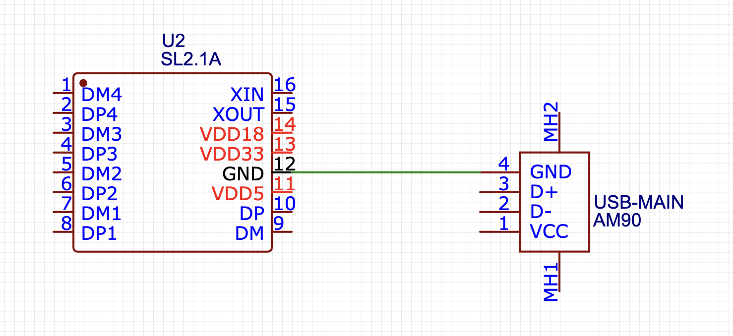
Now you can connect VCC on the usb to VDD5 on the chip. They aren't labelled the same thing, but VCC just means a voltage source, and USB-A is a 5V source.
Next up, connect D+ on the usb to DP on the chip, and D- on the usb to DM on the chip.

Hmmmm, this is looking a little like a bowl of spaghetti. Let's clean it up with nets!

Nets
Nets are a way to group together wires that are connected to eachother. They're a great way to make your schematic look cleaner and easier to read. Go ahead and remove the VCC & GND lines, then choose the GND net from the toolbar on the right.

Connect the GND net to the GND pins on the USB-A and the CoreChips SL2.1A. See how clean that new wiring is?
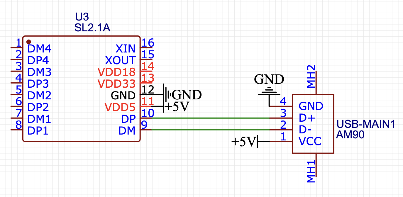
Nets are kinda like portals– you can connect them from a distance as a way to keep from crossing your wires on your schematic. They're also good for connecting lots of things together– we're going to need to wire a lot of things to GND in a sec, and nets are a great way to do that.
Keep in mind though with nets, there are a lot of ways to write things. All the following are a way to say PIN 4 and PIN 5 are connected to GND:

To prevent mistakes, try to keep your nets looking like mine for this tutorial, but in general everyone has their own style and that's ok.
Ground the Shield
Go ahead and connect MH1 & MH2 to GND also. These aren't really ports- they're just the parts where the metal cover of the USB sticks into the board. We'll connect them to ground in case there's any static electricity.
Add the other USBs
Next up let's connect the other USB-A connectors!
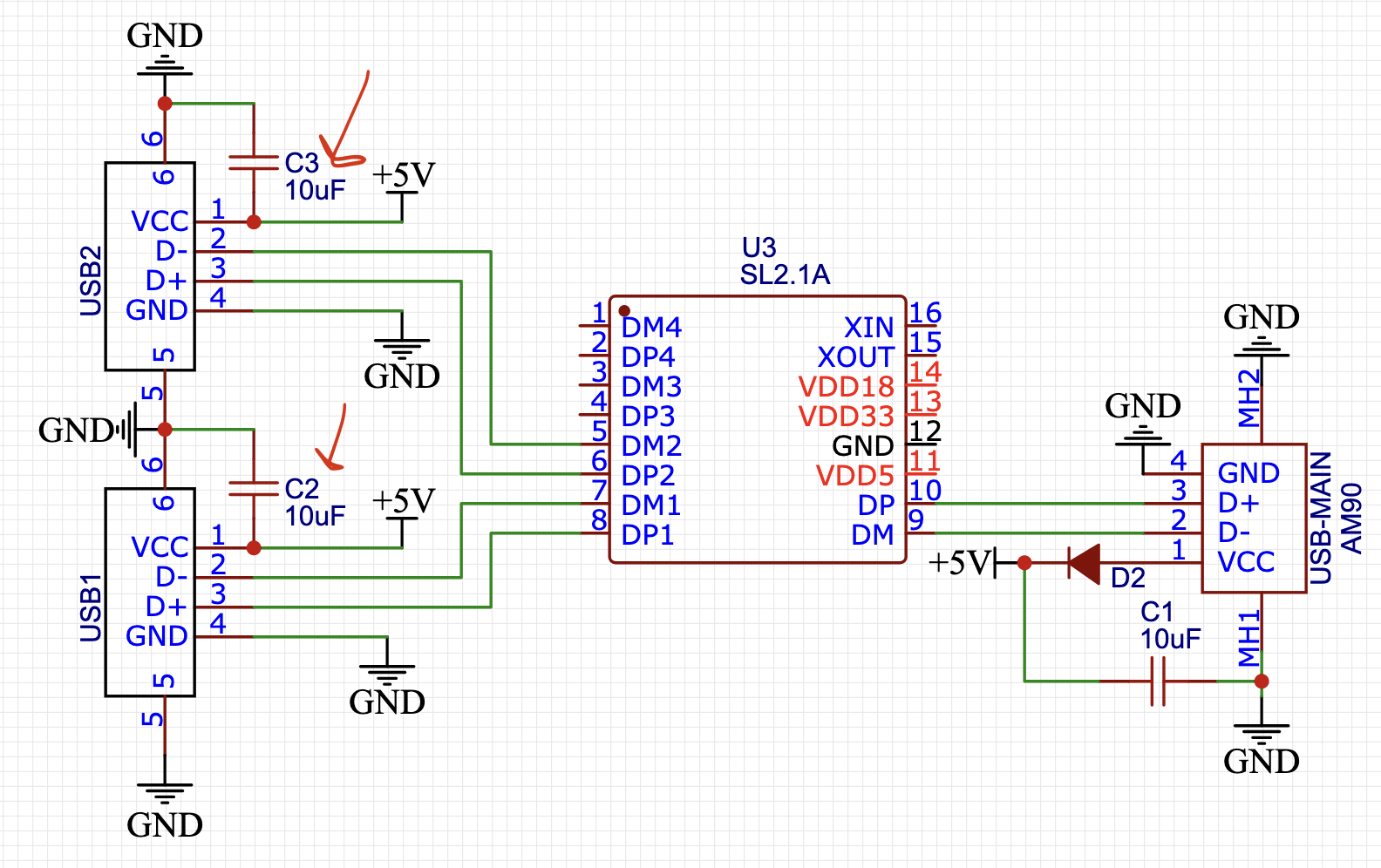
I'll position my USB-A female ports and hook them up to the main chip's DP and DM pins. DP1 goes to USB-1's D+. After getting the data lines wired, we'll connect the power using nets!
On these USBs, ports 5 & 6 are the same as ports MH1 & MH2. They're just the metal shield, so we'll connect them to GND as well.
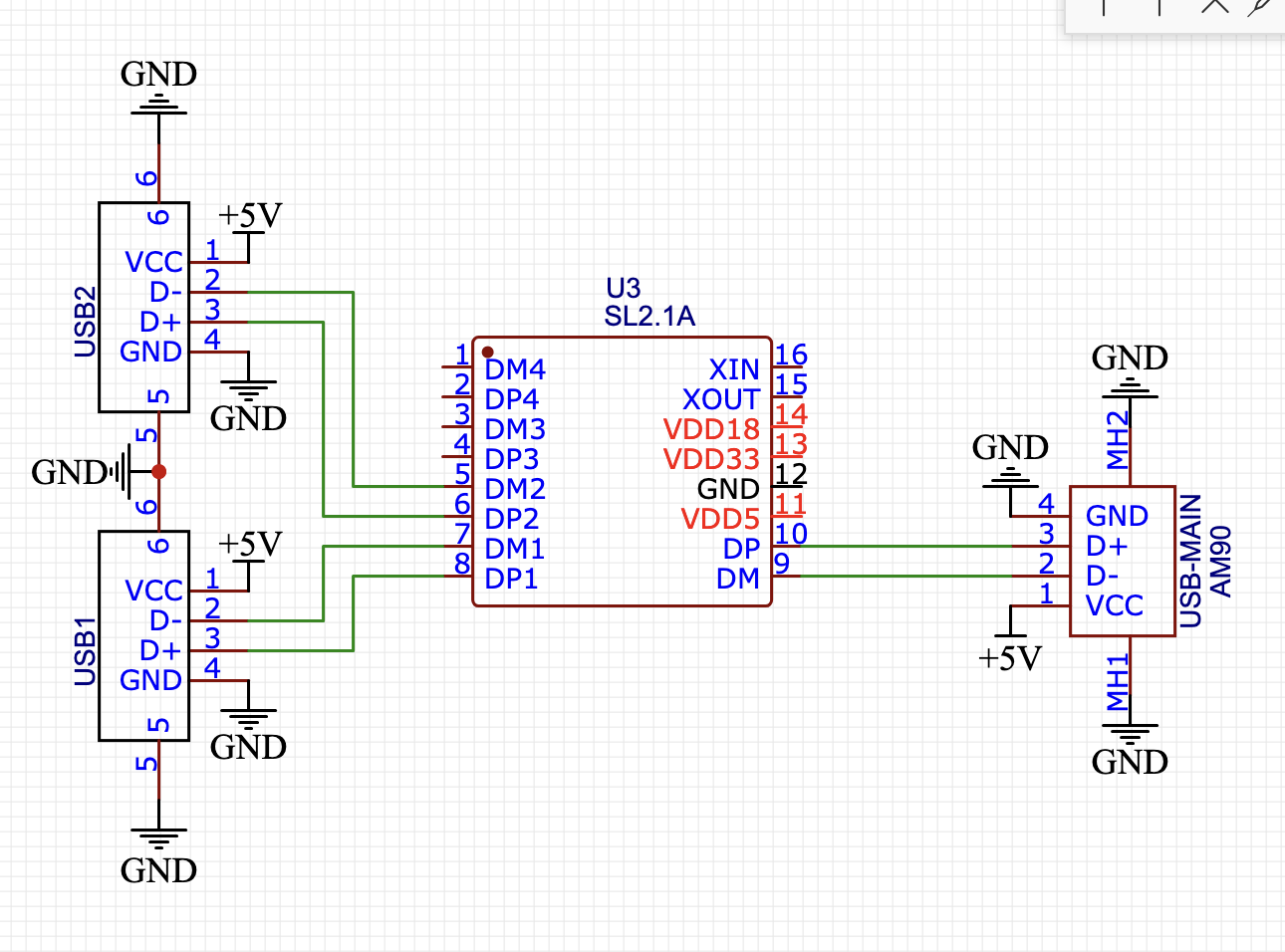
Remember, with nets you can connect from a distance!
Power surges
The design is almost complete, and in a perfect world it would work just fine. But we aren't in a perfect world- we live in a world with static electricty and power surges. We'll need to now protect our circuit. If we don't, we could fry our hub or even our computer's USB port!
Knowing where these protective components go can be an art and hotly debated on many stackoverflow forms. Fortunately, the spec sheets we're using contain some example circuits for us to use. Let's take a look at the CoreChips SL2.1A spec sheet again:
This is a little hard to see, so we'll go through it step by step. For now, just know we're getting the following instructions from reading this image & adapting it a little for our own design.
First up we'll add a diode to protect from a surge coming from the laptop. That's a case where the laptop sends too much power and goes beyond the 5V we want. The Schottky (pronounced "shot-key") diode with part number C48192 is perfect for this. Let's drop it in right after we take on the 5V power from the USB-A male.
Diodes ensure power flows in 1 direction. We don't want an accidental spike to flow back into our laptop! This Schottky diode will also slightly resist the flow of electricity, which is good for protecting against power surges.
Now let's protect from power surges that make it past the diode. We'll use a capacitor for this– it's kinda like a resevior for power. It can store up power and then release it when it's needed. If there's a power fluctuation, this capacitor will let the extra power blead out to GND harmlessly. We'll use a 10uF capacitor with part number C19702. Let's drop it in right after the diode, and connect it to GND.

When using a capacitor to prevent overflows like this it's called a "decoupling capacitor". I'll admit I don't 100% understand why, but this won't short 5V to GND.
Go ahead and use the same capacitors to protect the other USB-A ports. You can copy & paste the components, and then move them into place.
Unused ports
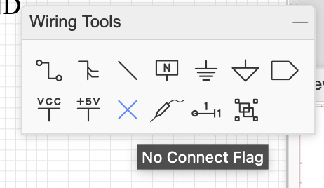
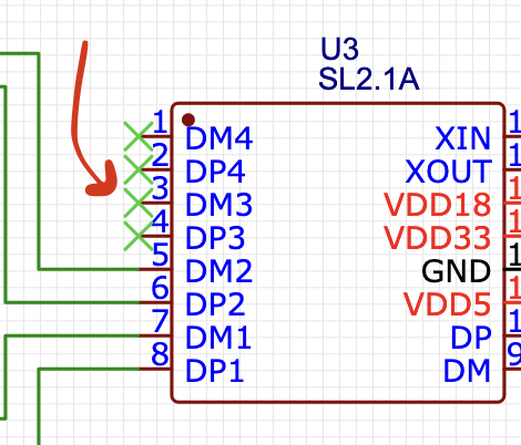
The SL2.1A chip we're using supports up to 4 USB ports, but we're making a smaller board for the tutorial so we won't be using the ports for "3" or "4". Go ahead and use the "no connection" tool to show in the schematic that these pins aren't being used.
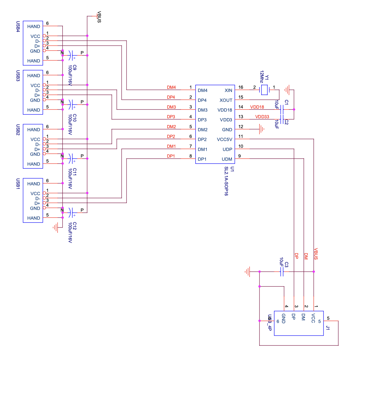
Making a 4-port USB hub is left as a challenge for you to do if you want to!
All finished should have pins connected to some label or wire, even if it's just a "no connection" symbol. Your PCB will error if you try to send it to the manufacturer with any pins unlabeled.
Next up are pins VDD33 and VDD18. Sometimes components will have these to provide lower voltages for their internal circuitry. We don't need to worry about them for this design, but the spec shows that we need to bleed off the power to GND using another 10uF capacitor.

Lastly, our chip provides clock circuitry through XIN and XOUT for advanced use if we wanted to overclock our USB ports. We aren't trying to do that, so we'll opt-out of it by connecting XIN to GND and marking XOUT as disconnected.
Now, let's check if all the pins are connected. Try converting the schematic to a PCB. If you see a warning pop up that means a net is missing or not connected. 
Finished!
If all the schematic is connected you've done it!

Now make your boardTake your board and build a working USB hub.
Now let's move into the PCB editor to make our board.
Congratulations! 🎉 🎉 🎉If you're a highschooler who enjoys programming or tinkering with hardware, make sure to join Hack Club, the world's largest nonprofit empowering teenagers to make cool projects! There's tons of programs where you can get prizes for programming, get your hardware projects fully funded and you can join the awesome community of 100k+ teenagers who love making cool stuff (just like you!).