Turn your blueprint into a board and order it!
If you haven't built a schematic yet, do so in part 1. Just in case you can start with the Schematic and the EasyEDA source we're starting with. Want to see the final result of this project? Here's a link to the final EasyEDA Design
Building the board!
Now that we have our schematic, let's turn it into a board!
Our starting schematic should look like this: 
This is what we're going to make: 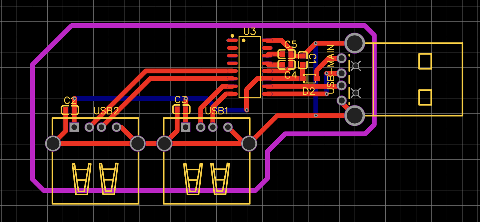
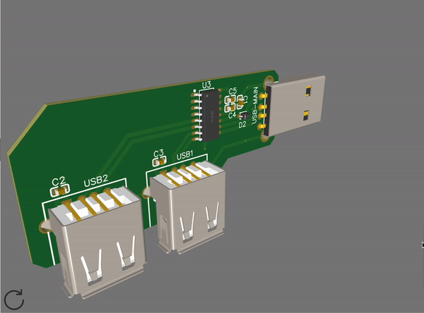
Once it's ordered, it'll look like this: 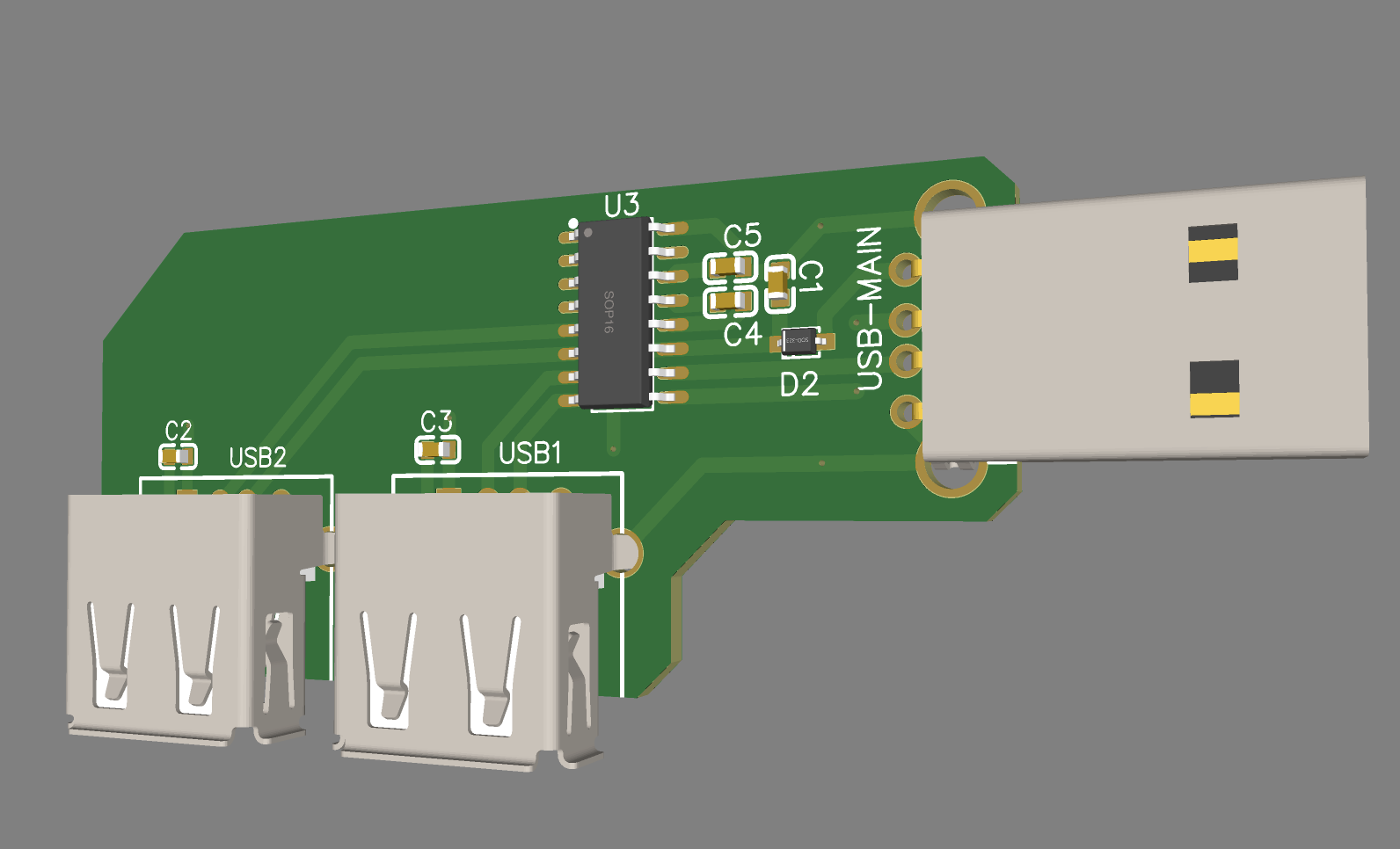
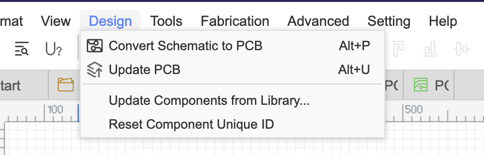
Step 1: Convert the schematic to a board
Click "Design > Convert to PCB" in the top right corner of EasyEDA. This will open up the board editor.
Next, confirm all the settings are exactly the same as– JK! these settings don't matter, just hit "apply" and move on:

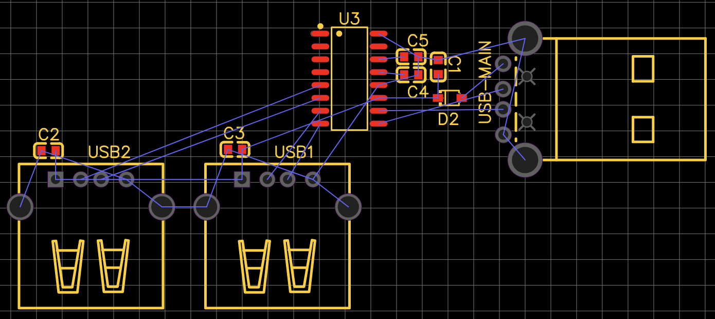
We'll be confronted with our parts laying out in the editor kinda like when we started out with the schematic. We'll need to move them around to make them fit on the board.

Step 2: Move the parts around
We want our parts to be generally close to what they should be connected to before connecting everything all together. This will make it easier to route the traces (fancy phrase for "wire it all up") later.
We've got a handy little tool to help us figure out our positions though! Rat lines! These are the little blue lines that connect the pins of our parts together. We can use these to figure out where to put our parts.
This is generated from our schematic, and is why we built our schematic first! If one of the blue lines ends up looking wrong it's usually because we're missing something in our schematics.
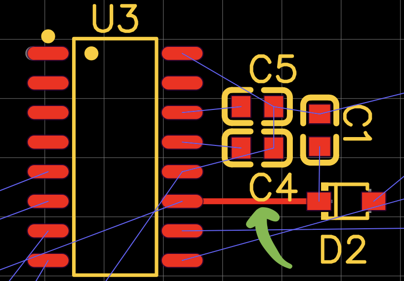
I moved the parts around a bit and ended up with this. A few things still overlap, but for the most part the lines have a clear route:
Keep in mind you might need to rotate your parts. Go ahead and do it with the "R" key. You can also rotate by degrees in the "Rotation" field on the right toolbar.
Step 3: Route the traces (wire up the dots)
Next up comes the fun part! Let's wire up our parts. This is more of an art than a science, but I recommend a couple tips:
- Do
GNDlast. It's very important, but the easiest to do. - You don't have to finish everything in one go. It usually takes a couple passes to get everything right & you'll end up with a better design if you don't force it all in one go.
- Don't be afraid to move your parts around if you need to.
First I'll select the "Track" tool on the toolbar:

I'm starting with the +5V trace in this example:
Lastly, this wire is a little thin for us, so let's embiggen it. Too small and the wire might burn out, but too big and it's hard to fit all your wires. There are a whole set of tables online that you can use to figure out the right width, but I usually just go with 0.8mm for my traces at +5V.
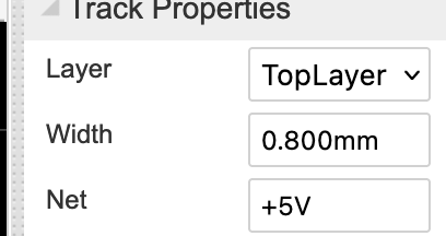

Technically, you can add an extra "c" to "thicc" for every 0.4mm of width.
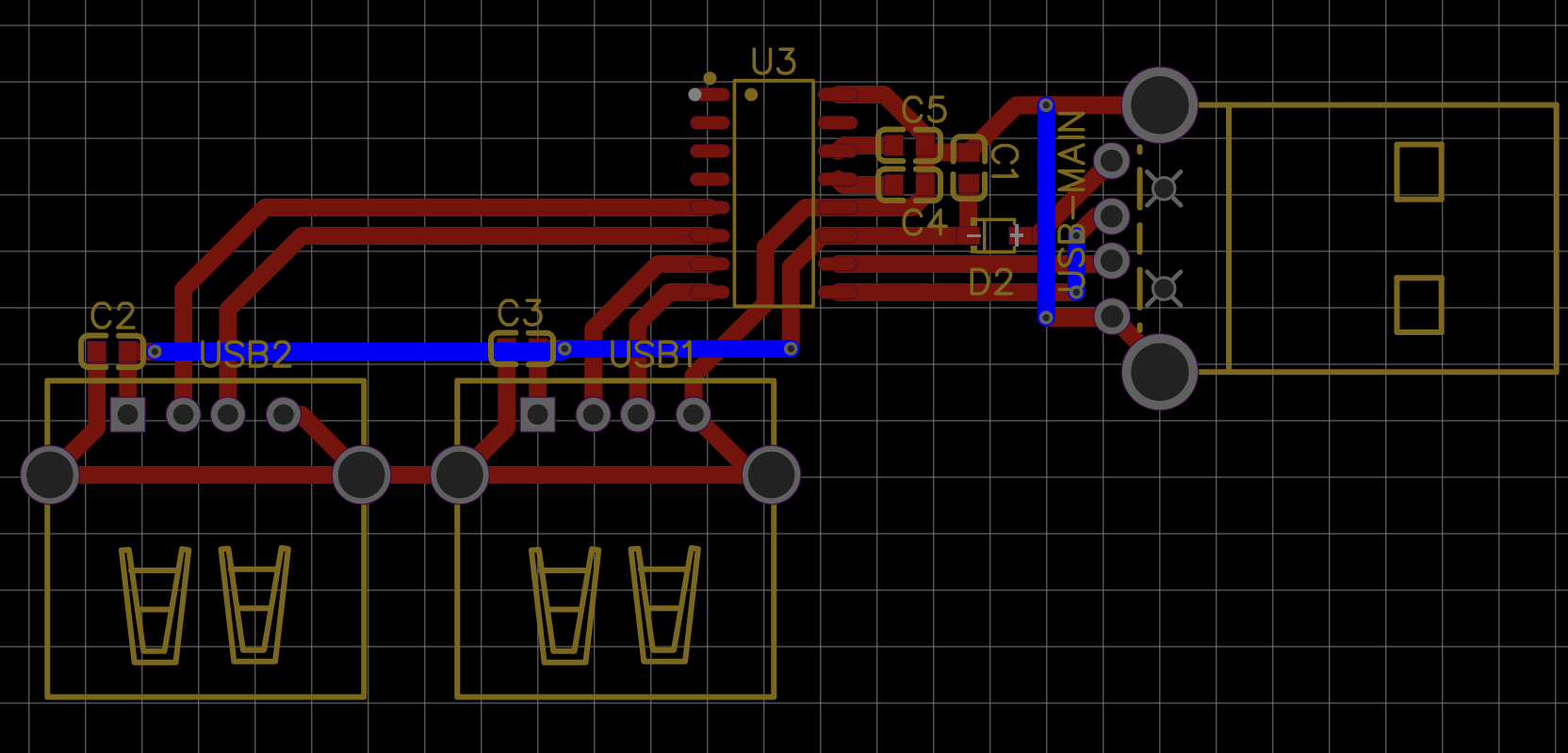
Take your time and route the traces you can. Here's how far I got after a couple passes:

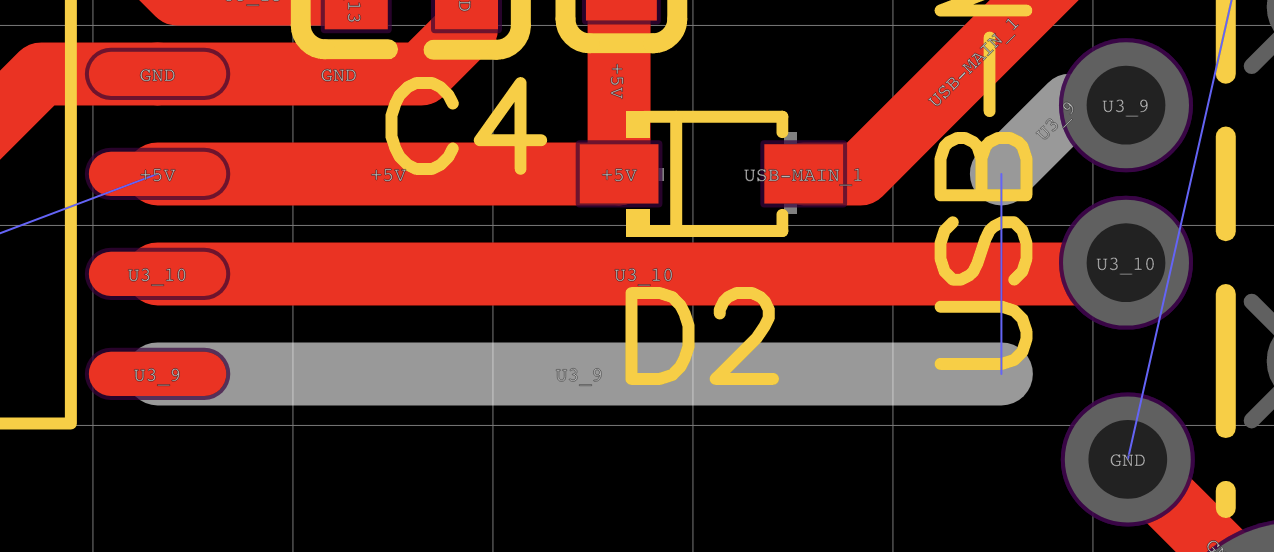
Notice that the +5V traces are still ratlined. I couldn't connect them without overlapping other traces, so I've left them unrouted for now. There's also part of the GND line that isn't connected yet.
Step 4: Oh, how the turn tables!
Now we need more space to route our stuff! Let's break out our superpower– the other side of the board!
That's right- the other side of the board can have a trace too! Some boards are pancaked together and have 4, 6, even 16 layers of traces! We're not going to be that fancy with this though– we can get away with just 2 layers for this project. Good for simplicity and keeping our costs down.
Let's use this tool to route the D- (for some reason showing up as U3_9 in my screenshot) pin for the USB-A male.
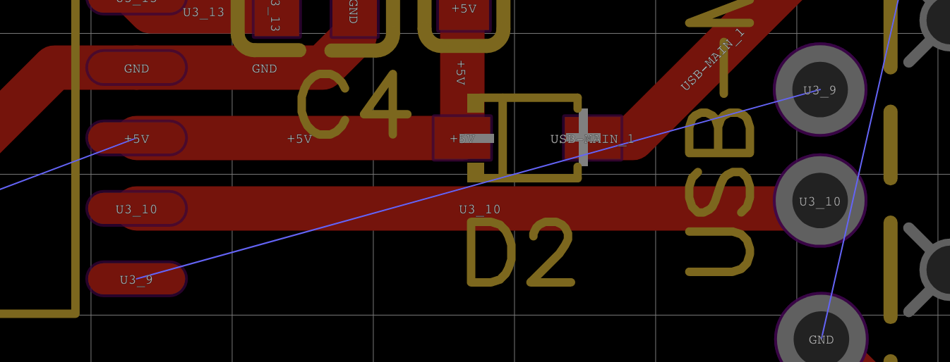
Add some traces to get the U3_9 line as close as it can without overlapping anything.
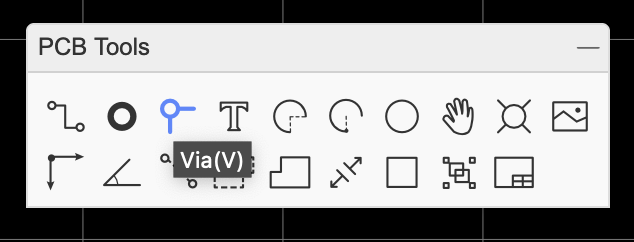
Switch to the "Via" tool and click the tip of the traces to add them to the tips. A "Via" is just a fancy way to say we're poking a whole through the board to the other side that's coated in copper so the current travels through it.

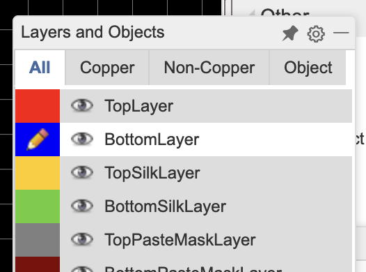
To switch to the other side of the board, click the "edit" icon next to "BottomLayer" on the layer toolbar. It should look like a pencil
Now we can route our traces on the bottom layer. Go ahead and connect the 2 vias we just made:
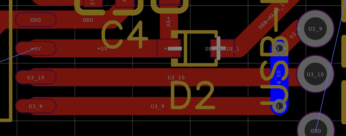
Nice! Now the ratline has disappeared- that means we're all done with those pins!
Try doing the rest of them on your own before continuing. Or don't... I'm just text on a website, I can't stop you from scrolling down to see the finished version.
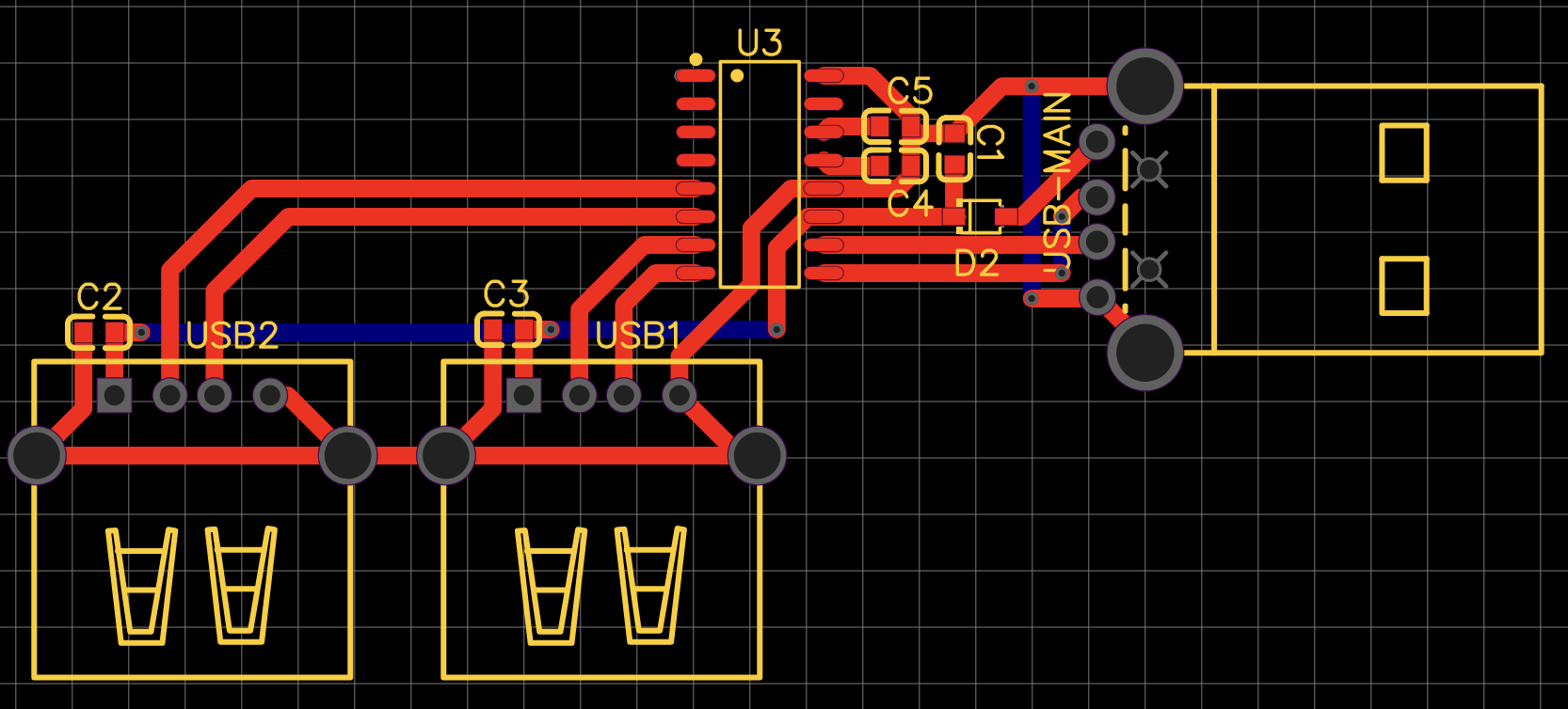
I had to add some more traces on the "TopLayer" to get all my "BackLayer" pins to connect.
Step 5: Cut that out!
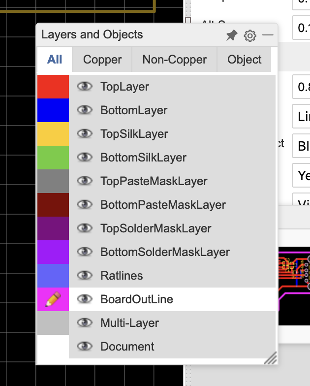
Next up we'll need to cut out our board and give it a shape! We'll use the "BoardOutline" layer to do this. Weirdly enough, we'll still be using the route tool like before.
You might already have a pink rectangle lying around from when you first imported your board from your schematic. Go ahead and delete that, we're making our own outline. A better outline!
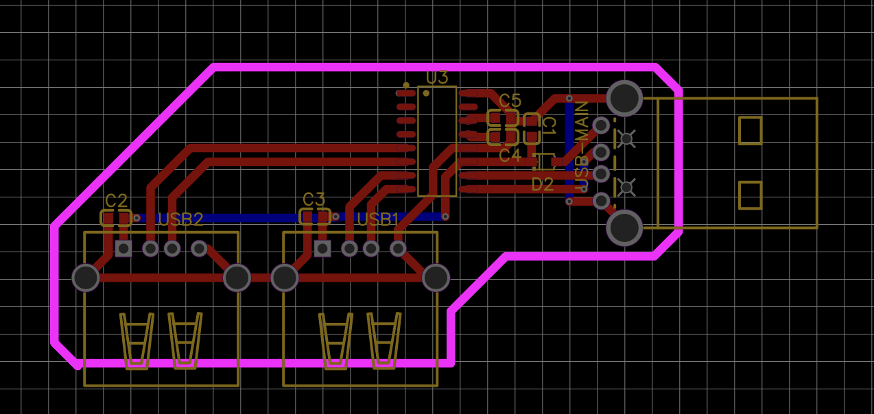
If your male USB port has a pink line in the footprint, make sure it's outside of the board outline. Some USB ports are "sink components," which means that they go below the board. This makes sure to give them ample room.
I made my trace look like this, but yours can look different! Just make sure that it's a closed shape and has enough padding around the edges that we don't trim of anything important. Sometimes the cutting machine will be a little off, so it's good to have a little extra space on the sides.
Also, don't forget to even out your corners!

Now that we have the borders cut out, let's see the results! Click "View > 3D View" in the top toolbar.


Done! That's it. You don't have to go home, but you can't stay here.
Congratulations! 🎉 🎉 🎉If you're a highschooler who enjoys programming or tinkering with hardware, make sure to join Hack Club, the world's largest nonprofit empowering teenagers to make cool projects! There's tons of programs where you can get prizes for programming, get your hardware projects fully funded and you can join the awesome community of 100k+ teenagers who love making cool stuff (just like you!).